
Nonlinear Metasurfaces
Recently, nonlinear metasurfaces have attracted attention for their ability to generate and control nonlinear light with subwavelength-scale elements. Our group utilizes all-dielectric metasurfaces for a diversity of nonlinear experiments in the mid-infrared (MIR), with applications ranging from efficient optical harmonics generation (i.e. light with a multiple of the original frequency) to deeply-subwavelength ultrafast laser-machining.
Nonlinear Semiconductor-based Metasurfaces for High Harmonic Generation
In one application, our group exploits all-dielectric metasurfaces composed of silicon-on-sapphire or gallium phosphide for highly-efficient optical harmonic generation (HG). Our HG metasurfaces are periodic arrangements of semiconductor pillars that support localized Mie-type resonant modes typical of regular semiconductor nanoarrays. At resonance, the coupling of fundamental light to the metasurfaces increases significantly, leading to greater energy available for nonlinear processes and a much higher level of nonlinear generation. This coupling also alters the energy distribution of the electrons in the material, potentially with a time dependence, which can further enhance the emission of harmonics. This results in highly efficient third harmonic generation (THG) from an ultrathin system as well as higher-order harmonics generation (HHG) that are typically only obtained by gases, with potential uses in advanced laser or telecommunications systems.
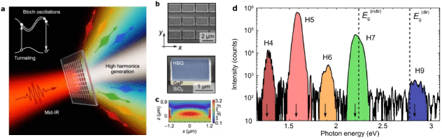
Figure 1: High Harmonic Generation with a resonant metasurface (a) Illustration of the high harmonic generation process: resonant GaP metasurfaces show efficient even and odd high harmonic generation (up to order H9). (b) Fabricated GaP metasurfaces: scanning electron microscope images, showing the substrate (SiO2), the antenna material (GaP), and the lithography mask (hydrogen silsesquioxane (HSQ). (c) Calculated local field map of the metasurface mode excited by a mid-infrared (mid-IR) pulse within the GaP antenna revealing an electric dipole mode. (d) Multi-pulse HHG spectra of the resonant sample. Arrows indicate the predicted HHG wavelengths.
Selected publications:
[1] Shcherbakov, M. R., Zhang, H., Tripepi, M., Sartorello, G., Talisa, N., AlShafey, A., … & Shvets, G. (2021). Generation of even and odd high harmonics in resonant metasurfaces using single and multiple ultra-intense laser pulses. Nature communications, 12(1), 4185.
[2] Shcherbakov, Maxim R., et al. “Photon acceleration and tunable broadband harmonics generation in nonlinear time-dependent metasurfaces.” Nature communications 10.1 (2019): 1345.
Subwavelength fs-Laser Nanomachining using Silicon-Metasurfaces
Additionally, our group combines ultrafast high-intensity laser pulses with localized hotspots within nanostructures to perform nanoscale machining with precise control over laser-induced damage. Usually, laser-induced damage is an undesired effect in fs-laser experiments, arising from localized high field concentrations within resonators. We exploit this effect in square resonators with triangular notches. By design, the metasurface resonates near the laser wavelength and exhibits nonlinear photoinduced free carrier production. Illuminating the Si-resonators with few-pulse trains below the single-pulse damage threshold facilitates localized phase explosions and gradual volumetric material ablation at the notch position, where the field intensity is the highest. While laser-machining approaches are typically restricted by the diffraction limit to yield a smallest resolvable dimension equal to half the laser wavelength, our results show deeply-subwavelength-scale (80) modifications to Si-based resonators illuminated by fs laser pulses. By varying the laser pulse intensity, polarization, and number, we demonstrate nanostructuring with polarization-controlled orientation and variable widths and lengths.
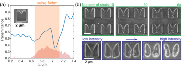
Figure 2: Semiconductor-Metasurface-Assisted fs–Laser-Machining. (a) Experimental transmission spectra of the metasurface (solid line). Inset: Scanning electron microscope image (SEM) of the M-shaped microresonator unit cell; red-shaded area: incident laser intensity spectrum; orange rectangle: FWHM of the incident pulse’s intensity spectrum. (b,c) SEM images of microresonator arrays exposed to 7um laser pulses with (b) increasing shot-numbers and constant intensity and (c) increasing intensity and constant shot-number.
Selected publications:
[1] Shcherbakov, Maxim R., et al. “Laser nanostructuring by tailored free carrier generation in designer semiconductor metasurfaces.” CLEO: Science and Innovations. Optica Publishing Group, 2021.