
Electron beam moving inside the gap can excite SPhPs (surface phonon polaritons) at the SiC-vacuum interface because the dielectric permittivity of SiC is negative within the infrared reststrahlen band. Two modes: (i) accelerating and (ii) deflecting modes will be excited, and they are both Cherenkov-type emissions.
The accelerating wakes excited by a relativistic driver bunch can be used to accelerate a trailing bunch to hundreds of MeV. High accelerating gradients are expected, one pC driver produces 120 MeV/m accelerating field in 10 μm gap, and 220MeV/m in 6 μm gap.
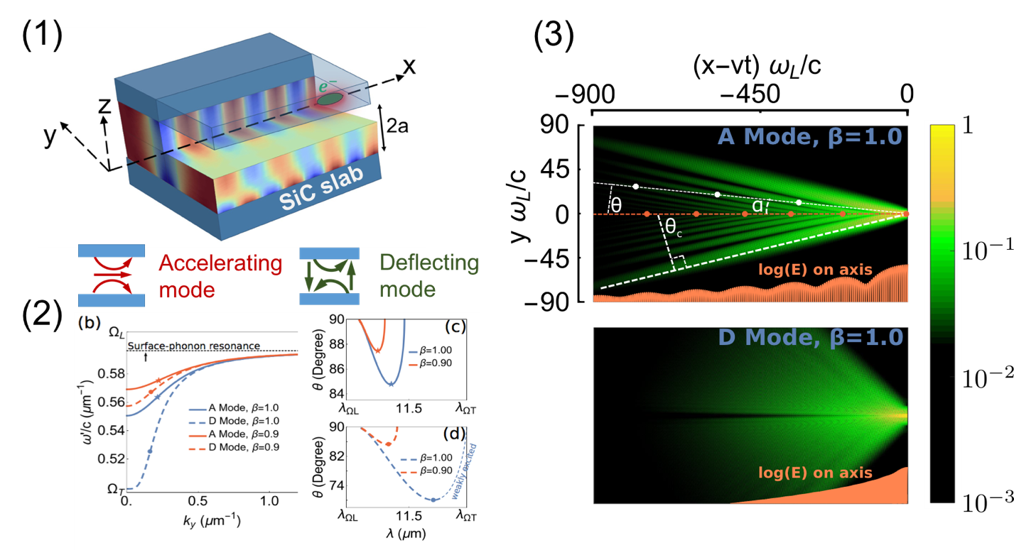
Figure 1. (1) The schematics of SWABSiC and beam-excited surface wave; (2) The dispersion relations of surface modes; (3) The Cherenkov-type wakefields excited by ultra-relativistic electron beam.
We have proposed to use a modulated electron bunch to excite the accelerating wakes. The bunch will be prepared by an undulator at right frequency to resonantly interact with the SPhPs modes, accelerate the trailing part and produce a high energy spectrum tail.
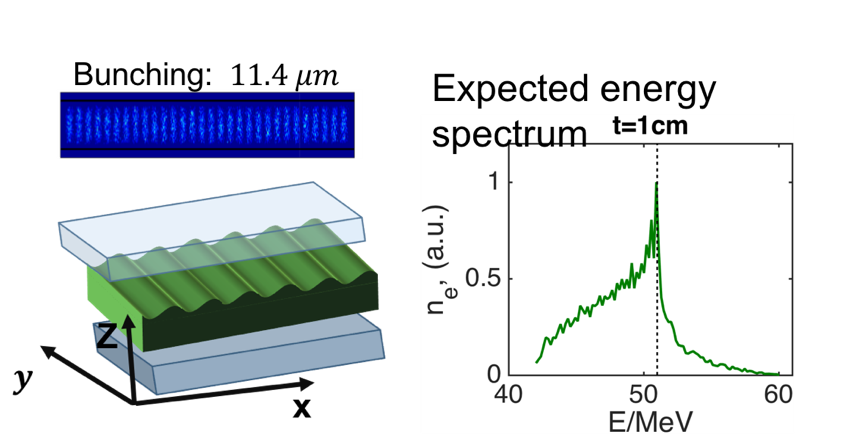
Figure 2. (1) Schematic of wakefield acceleration. (2) Expected energy spectrum after a 300 pC modulated beam propagates 1 cm in SWABSiC.
Electron Beam Throughput Test in ATF BNL
To investigate the proposed concepts, the SWABSiC structure is planned to be tested with electron beam at the Accelerator Test Facility in Brookhaven National Laboratory. The new structure, as shown in the bottom-left inset of Fig. 1, has been fabricated with smaller physical dimensions as following. A layer of 1.4 µm thick silicon carbide thin film is epitaxially grown on two 10 mm×15 mm×5 mm Si bricks. To precisely control the separation between two SiC interfaces, a pair of spacers are deposited by spin-coating a 9µm layer of photoresist SU-8 on one of the Si bricks as the two triangular areas in the picture. Therefore, the accelerating channel of the new sample is larger than the original structure [4]. The two pieces of Si bricks are loaded on aluminum braces separately and tightly sandwiched together by two retention rings in a 1-inch lens tube which is fixed to a mirror mount for aligning the structure to the electron beam path.
The throughput measurement of the new SWABSiC structure using the electron beam is performed within the Electron-Plasma chamber in beam line #2 at ATF. The schematic of the experimental setup in the chamber is shown in Fig. 1. The relativistic electron beam is prepared with initial energy of 57 MeV and total charge of 300 pC. In the chamber section, the beam is focused and shaped by the quadrupolar magnet (QPM) and the beam profile is observed by a phosphor screen co-aligned with the front surface of the SWABSiC structure. The accelerating channel of the sample is aligned to the beam line HeNe laser with the sample assembly mounted on a movable stage granting the capability of either keeping the beam path clear or inserting the structure into the beam path. The beam profile monitor (BPM) #7 is located at downstream of the sample assembly providing the optical images of transmitted beam. The amount of transmitted charges is determined by summing over pixel values in the area of interest as indicated as the red circles in the Fig. 2. The transmitted charges are defined as Qfull-beam for the beam path is clear and QSWABSiC for the structure is inserted into the path. The throughput is then calculated from following formula,

The resulting throughput rate of the circular beam profile in Fig. 2a is 9.44% while this rate can be improved to 12.12% by shaping the beam into the elliptical profile as in the Fig. 2b to match the cross-section of SWABSiC accelerating channel. One thing to clarify at this point is that the total charge of the full-beam is directly measured from the ammeter downstream when the structure is not in the beam path while the charge of the transmitted beam is derived from the throughput rate times the total charge since the electron beam is diverged after passing the structure and cannot be collected by the energy spectrometer.
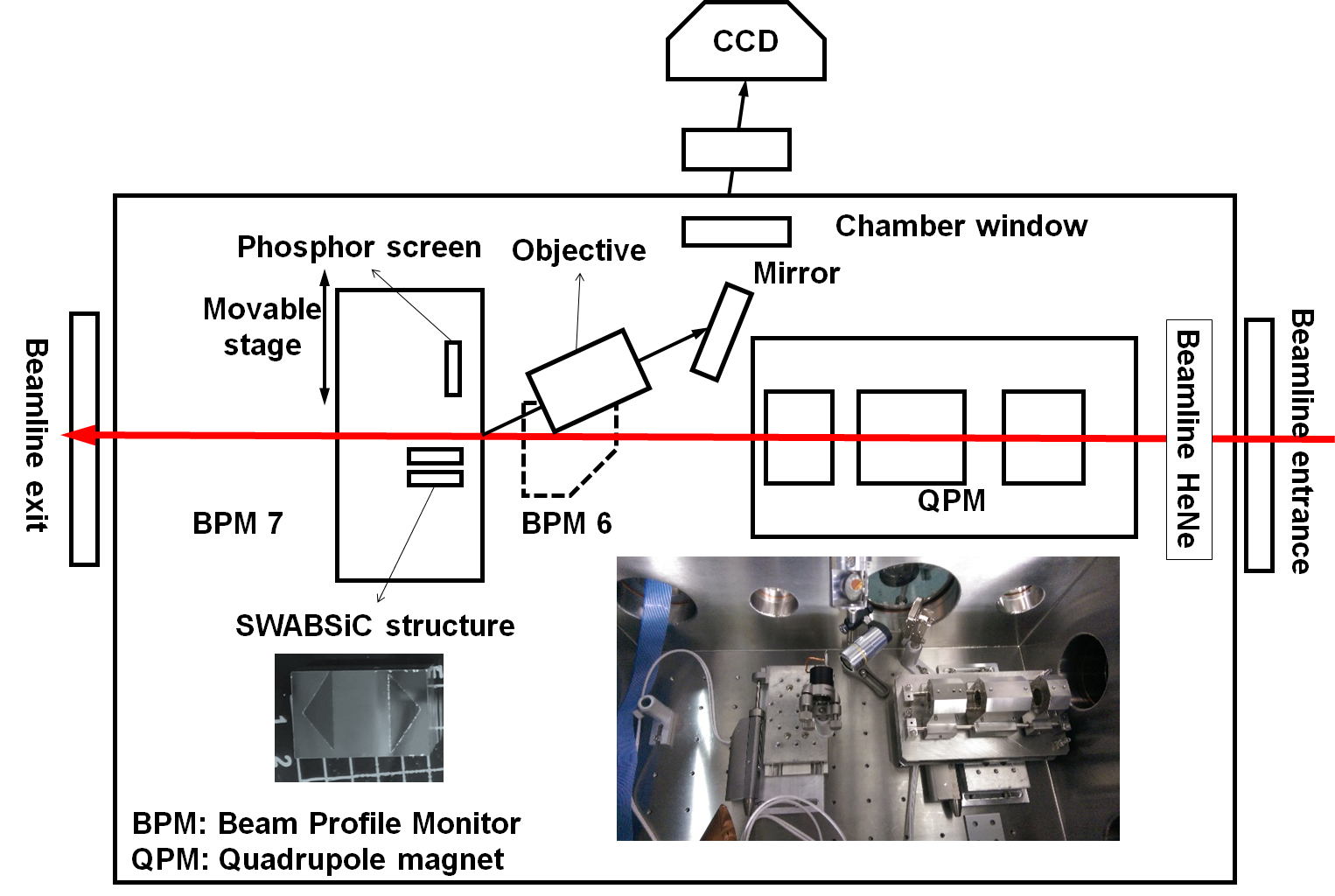
Figure 1. Schematic of the electron beam throughput experiment of SWABSiC structure at ATF BNL. Bottom-left inset: top view of the newly fabricated SWABSiC structure with 2 triangular spacers made of SU-8 photoresist; bottom-right inset: picture of the actual experimental setup in the Electron-Plasma chamber in beam line #2.
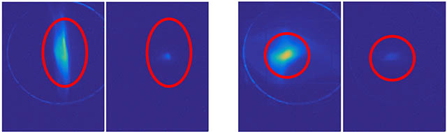
Figure 2. CCD images of transmitted charges on BPM for (a) circular beam profile and (b) elliptical beam profile. In both cases, the left image is for the full-beam without structure in the path while the right image is for the structure inserted into the path. The resulting throughputs are calculated as 9.44% and 12.12% for circular and elliptical beam profile respectively.
Relevant Publications:
Burton Neuner III, Dmitriy Korobkin, Gabriel Ferro, and Gennady Shvets, “Prism-coupled surface wave accelerator based on silicon carbide,” Phys. Rev. ST Accel. Beams 15, 31302 (2012)